n型基板
 (217KB)
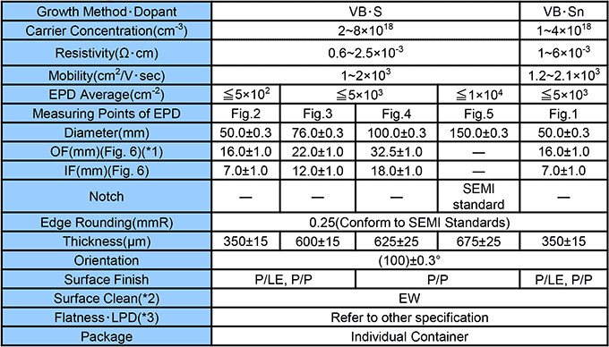
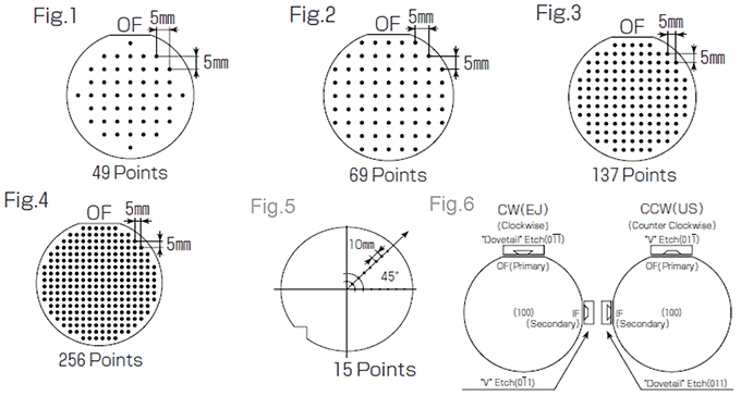
Standard Specifications
Notes
(*1) High Precision OF(±0.02°) is available.
(*2) EW : Etched Wafer
(*3) LPD : Light Point Defects
Attached Data
- Standard
- :
- Resistivity・Mobility・Diameter・OF・IF・Thickness (min.~max.)
EPD Map
- Option
- :
- Accuracy of Orientation・Flatness・Light Point Defects